Patent
2021 .Title of invention
Application Date (Issue Date): 2021.12.13
Application Number (Patent Number): 10-2021-0177394
Status: 특허
Applicant: 울산대학교 산학협력단
Inventor: 김용수,라시드 마문 우르,타히르 지샨
2021 .Title of invention
Application Date (Issue Date): 2021.11.17
Application Number (Patent Number): 10-2021-0158148
Status: 특허
Applicant: 울산대학교 산학협력단
Inventor: 김태헌,안창원,시라즈무함마드
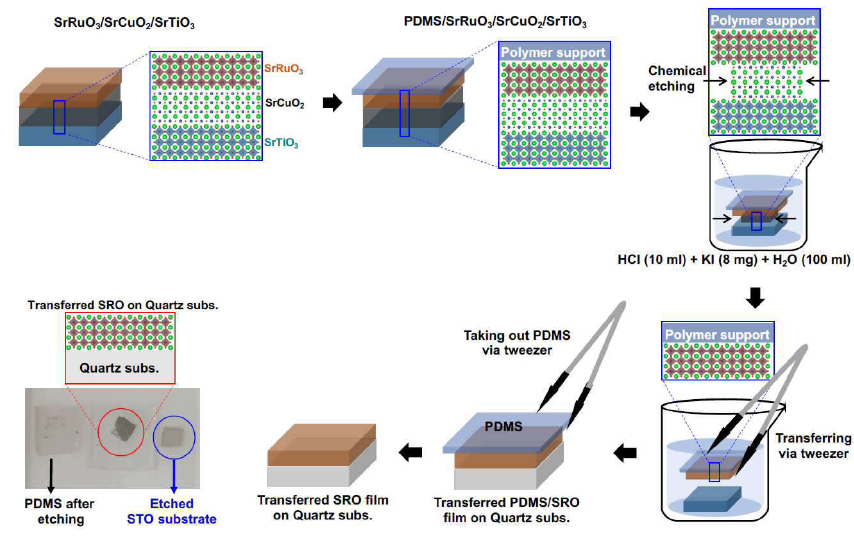
2021 .Title of invention
Application Date (Issue Date): 2021.5.27
Application Number (Patent Number): 10-2021-0068012
Status: 특허
Applicant: 울산대학교 산학협력단
Inventor: 김태헌,안창원,조재훈,최진산,김일원
2021 .Title of invention
Application Date (Issue Date): 2021.5.21
Application Number (Patent Number):10-2021-0065598
Status: 특허
Applicant: 울산대학교 산학협력단
Inventor: 홍순철,투무르바타르 체베르,도르쥐 엇후,도르쥬렌 툽신
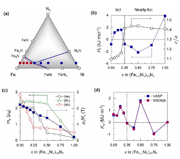
2021 .Title of invention
Application Date (Issue Date): 2021.03.24
Application Number (Patent Number): 10-2021-0037650
Status: 특허
Applicant: 울산대학교 산학협력단
Inventor: 조신욱,쩐 홍 냔
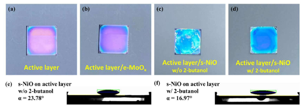
2021 .Title of invention
Application Date (Issue Date): 2021.1.21
Application Number (Patent Number): 10-2021-0008548, PCT/KR2021/001242
Status: 특허
Applicant: 울산대학교 산학협력단
Inventor: 조성래,박은정,박은지
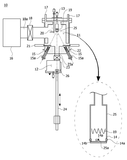
2021 .Title of invention
Application Date (Issue Date): 2021.1.21
Application Number (Patent Number): 10-2021-0008549
Status: 특허
Applicant: 울산대학교 산학협력단
Inventor: 조성래,박은정,박은지
2021 .Title of invention
Application Date (Issue Date): 2021.1.20
Application Number (Patent Number): 10-2021-0007863, PCT/KR2021/001251
Status: 특허
Applicant: 울산대학교 산학협력단
Inventor: 김용수,김성도,타히르 지샨
2021 .Title of invention
Application Date (Issue Date): 2021.04.06
Application Number (Patent Number): 10-2238865
Status: 특허
Applicant: 울산대학교 산학협력단
Inventor: 조신욱, 쩐홍냔

2020. Title of invention
Application Date (Issue Date): 2020.07.17
Application Number (Patent Number): 10-2137238
Status: 특허
Applicant: 울산대학교 산학협력단
Inventor: 김태헌, 안창원, 김일원, 시라즈 무하마드
2019. Title of invention
Application Date (Issue Date): 2019.10.28
Application Number (Patent Number): 10-2039748
Status: 특허
Applicant: 울산대학교 산학협력단
Inventor: 김용수, 최학순

2018. Title of invention
Application Date (Issue Date): 2018.09.27
Application Number (Patent Number): 10-1903991
Status: 특허
Applicant: 울산대학교 산학협력단
Inventor: 김용수, 윤종원
Application Date (Issue Date): 2018.05.04
Application Number (Patent Number): 10-1857387
Status: 특허
Applicant: 울산대학교 산학협력단
Inventor: 김정대, 김상화
2017. Title of invention
Application Date (Issue Date): 2017.06.28
Application Number (Patent Number): 10-1753980
Status: 특허
Applicant: 울산대학교 산학협력단
Inventor: 조성래,권해웅,반 쾅 웬,박은지,박은정,김말식

Application Date (Issue Date): 2017.04.06
Application Number (Patent Number): 10-1726498
Status: 특허
Applicant: 울산대학교 산학협력단
Inventor: 조성래,신유리미,반 쾅 웬,안 투안 둥

Application Date (Issue Date): 2017.06.15
Application Number (Patent Number): 10-1749859
Status: 특허
Applicant: 울산대학교 산학협력단
Inventor: 김정대, 김태훈
2014. Title of invention
Application Date (Issue Date): 2014.04.30
Application Number (Patent Number): 10-1393096
Status: 특허
Applicant: 울산대학교 산학협력단
Inventor: 한성홍, 김순욱, 느구옌 트리 코아
Abstract: :
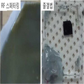
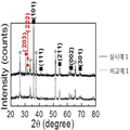
The present invention relates to a manufacturing method and a graphene oxide thin film of the graphene oxide thin film using an RF magnetron (Radio Frequency Magnetron) sputtering, and sputtering of a graphite target oxide using RF magnetron sputtering method, an oxide thin film directly graphene It is possible to manufacture a thin film having excellent quality by a simple process and an easy operation without being harmful to the human body, and it is economical because the cost and the apparatus are relatively small. In particular, the thickness of the thin film can be freely controlled by adjusting the deposition time.
Application Date (Issue Date): 2014.10.14
Application Number (Patent Number): 10-1453150
Status: 특허
Applicant: 울산대학교 산학협력단
Inventor: 김일원, 안창원, 최강호, 원성식, 석해진, 채송아, 이순규, 장기봉
Abstract: :
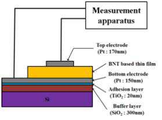
The invention Reactive Tempalted Grain Growth (RTGG) as method of producing a lead-free piezoelectric ceramic according to the method and relates to a lead-free piezoelectric ceramic produced thereby, (1-y) [( 1-x) Bi 0 .5 Na 0 .5 T i O 3 -xBi 0 .5 K 0 .5 TiO 3] -yBiAlO 3 (BNT-BKT-BA; x = 0~1.0, y = 0~0.1) powder and Na 0.5 Bi 4.5 Ti 4 O 15 (NBiT) particles were mixed with a solvent, a dispersant, a plasticizer and a binder by ball milling, A slurry producing step of producing a slurry; A deaeration step of de-airing the slurry by a vacuum pump to remove bubbles from the slurry produced, remove bubbles in the slurry during ball milling and increase viscosity; A tape casting step of making the defoamed slurry into a green sheet by a tape caster; A drying step of drying the prepared green sheet and removing the binder; A processing step of compressing and cutting the dried green sheet to make a BNT-BKT-BA ceramic having a constant thickness; A sintering step of sintering the processed BNT-BKT-BA ceramics; A lapping step of finishing the sintered BNT-BKT-BA ceramic by processing it to be thinner than in the processing step; And an electrode forming step of forming electrodes on both sides of the finished and finished BNT-BKT-BA ceramic, thereby obtaining a BNT-BKT-BA ceramic excellent in electric field induced deformation characteristics.
Application Date (Issue Date): 2014.07.18
Application Number (Patent Number):10-1423418
Status: 특허
Applicant: 울산대학교 산학협력단
Inventor: 김일원, 안창원, 아만울라, 최강호, 김희성
Abstract: :
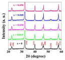
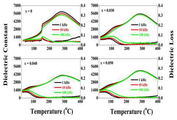
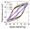
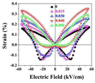
The present invention relates to a lead-free piezoelectric ceramic composition and, more particularly, to a lead-free piezoelectric ceramic composition formed by adding Bi(Mg,Ti)O3 to a ceramic composition with Bi0.5(Na,K)0.5TiO3. The lead-free piezoelectric ceramic composition according to the present invention is environmentally-friendly by providing a Bi-based piezoelectric ceramic material unlike existing lead-based PZT which is harmful to a human body and induces environmental pollution. A piezoelectric feature is improved by a high strain rate when an electric field is applied.
Application Date (Issue Date): 2014.05.15
Application Number (Patent Number):10-1398366
Status: 특허
Applicant: 울산대학교 산학협력단
Inventor: 한상욱, 황영훈, 박영신, 홍순철
Abstract: :
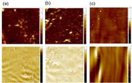
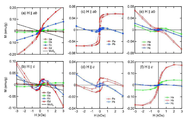
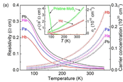
The present invention relates to a method for manufacturing a ferromagnetic single-crystal material and a ferromagnetic material produced by the method, and more particularly, to a ferromagnetic single-crystal material selected from the group consisting of MoS 2 , MoSe 2 , MoTe 2 , WS 2 and WSe 2 , Or a simple process of heat-treating in a hydrogen atmosphere, a ferromagnetic material having a ferromagnetic magnetic property at room temperature can be produced. By using the method of the present invention, it is possible to control the magnetic anisotropy parallel to or perpendicular to the crystal plane direction while imparting ferromagneticity to the monocrystalline single crystal material selected from the group consisting of MoS 2 , MoSe 2 , MoTe 2 , WS 2 and WSe 2 Whereby a ferromagnetic material having magnetic anisotropy parallel or perpendicular to the crystal plane direction can be selectively produced.

2013. Title of invention
Application Date (Issue Date): 2014.05.15
Application Number (Patent Number): 10-1306454
Status: 특허
Applicant: 울산대학교 산학협력단
Inventor: 김일원, 안창원, 원성식, 장기봉, 채송아, 이순규, 최해윤
Abstract: :
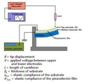
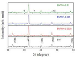
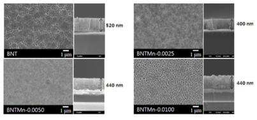
This invention relates to a method of making lead-free piezoelectric ceramic films. Specifically, the invention is directed to a method for fabricating lead-free piezoelectric free standing films having enhanced piezoelectric properties. The films may be used for a number of applications including incorporation in microelectronic devices such as energy harvesting devices and sensor technologies.

Application Date (Issue Date): 2013.09.09
Application Number (Patent Number): 10-1306472
Status: 특허
Inventor: 이재신, 김일원
Abstract: :
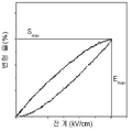
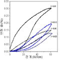
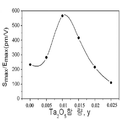
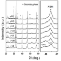
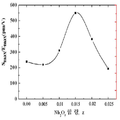
Ta 2 in the ceramic composition having a composition of x Bi 1/2 K 1/ 2 TiO 3 - the invention is lead-free piezoelectric relates to a ceramic composition and, more particularly (1-x) Bi 1/ 2 Na 1/2 TiO 3 The present invention relates to a lead-free piezoelectric ceramic composition characterized in that at least one metal oxide selected from O 5 , Nb 2 O 5 , ZrO 2 , HfO 2 and Y 2 O 3 is added. The lead-free piezoelectric ceramic composition according to the present invention is environmentally friendly because it provides a bismuth-based piezoelectric ceramic material, unlike conventional lead-based PZT, which is harmful to the human body and causes environmental pollution, and applies an electric field by adding a small amount of metal oxide. When exhibiting a high strain rate, there is an effect of improving the piezoelectric properties.
Application Date (Issue Date): 2013.12.27
Application Number (Patent Number): 10-1347889
Status: 특허
Inventor: 김용수, 이건희, 최학순
Abstract: :
The present invention relates to a graphene-based carbon material electronic device using a flexible substrate and a method for manufacturing the same, a flexible substrate; A drain electrode and a source electrode respectively formed on the flexible substrate; A channel layer formed between the drain electrode and the source electrode; A gate insulating layer formed on the channel layer; It includes; the gate electrode formed on the insulating layer, and simplify the manufacturing process to improve the workability, the flexible substrate can be used due to the low temperature process, not through the etching process not only shorten the work time but also reduce the manufacturing cost Let's do it.

Application Date (Issue Date): 2013.11.21
Application Number (Patent Number): 10-1333831
Status: 특허
Inventor: 김용수, 최학순
Abstract: :
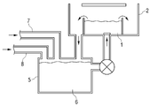
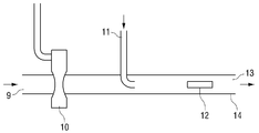
Disclosed is a surface treatment method of a semiconductor device. Surface treatment method of a semiconductor device for performing a dry cleaning by using a plasma, comprising the steps of generating a plasma by introducing a process gas containing hydrogen (H2) and xylene (SiH2) -based material to the plasma generator; And dry cleaning the surface of the silicon substrate of the semiconductor device using radicals activated by the plasma. This makes it possible to efficiently clean the surface of the silicon substrate.
Link : https://patents.google.com/patent/KR101333831B1/en

Application Date (Issue Date): 2013.11.01
Application Number (Patent Number): 10-1327072
Status: 특허
Inventor: 한성홍, 성승기, 김의정, 편민욱, 윤영민, 심창호, 지성진
Abstract :
The present invention relates to a method for forming a trap level and a method for manufacturing a photocatalyst thin film or a thin film solar cell using the same, and more specifically, electron recombination is formed by forming a trap level by injecting stress into a metal oxide or metal fluoride material having a band gap. The present invention relates to a method for forming a trap level, and a method for manufacturing a photocatalyst thin film or a thin film solar cell using the same. According to the manufacturing method of the present invention, it is possible to easily control the recombination of electrons by forming a trap level in a simple process of injecting stress into the metal oxide or the metal fluoride itself without a separate physical and chemical mixing process of the metal, the metal oxide or the metal fluoride. It has an effect.
Link : https://patents.google.com/patent/KR20110097429A/en
